A potassium-niobium crystal film on silicon could expand ways to control light
Researchers grew a high-quality electro-optic film on silicon, creating a possible new material platform for silicon photonics.
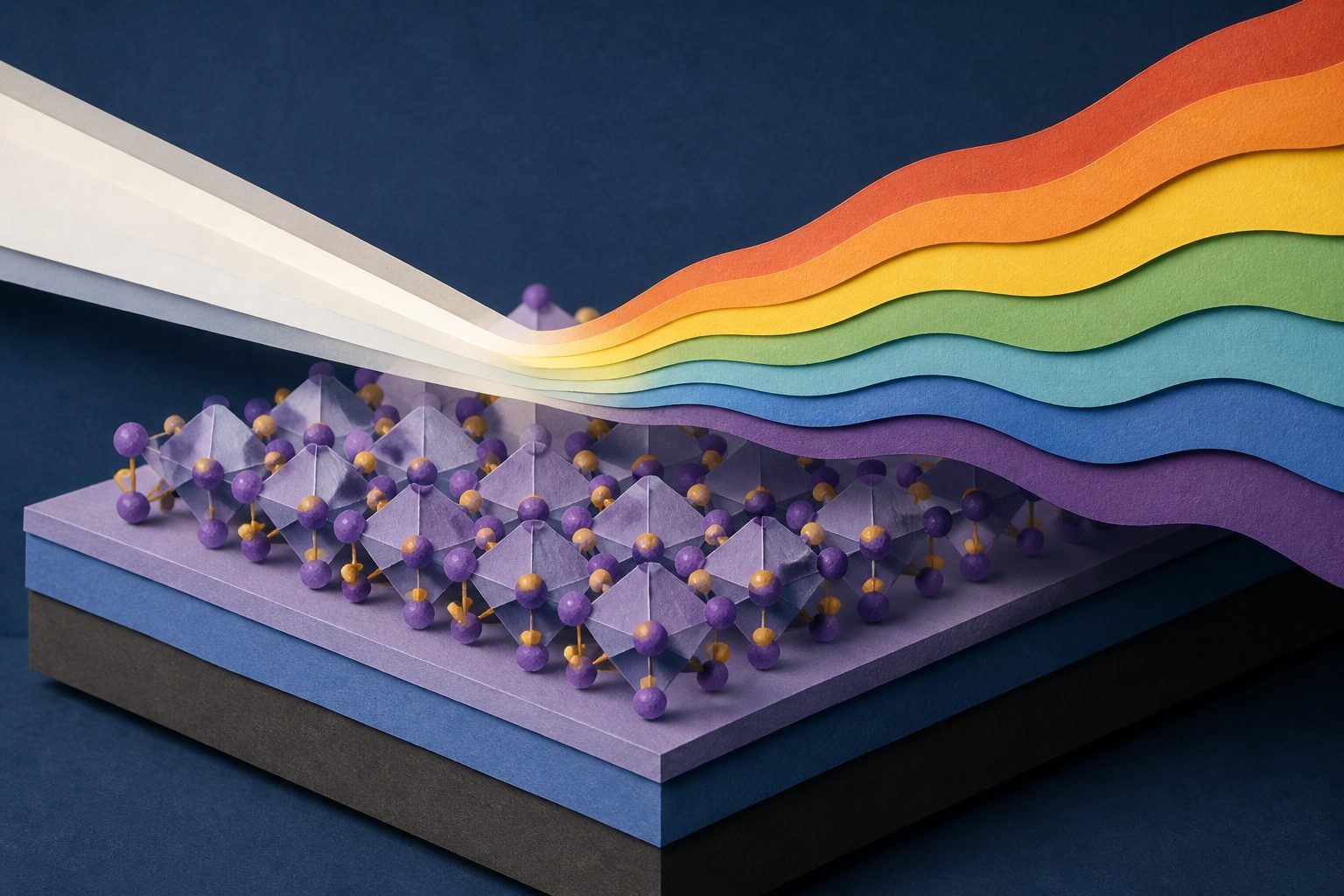
Editorial illustration — not from the study.
Silicon is widely used in photonics but does not naturally change its optical properties in response to an electric field. Researchers integrated the ferroelectric material potassium niobate, also called KNbO3, directly onto silicon using a controlled growth process designed to prevent potassium from escaping.
Measurements and microscopy indicated that the films were phase-pure, epitaxial and separated from the silicon by sharp interfaces. The films showed structural changes similar to those in KNbO3 crystals and had an effective electro-optic response of 146 ± 14 picometers per volt at 1550 nanometers.
What the film showed
The study reports the first epitaxial integration of KNbO3 thin films on silicon. The researchers used suboxide molecular-beam sources, in situ monitoring and thermodynamic simulations to identify a growth window that produced phase-pure films despite potassium's volatility.
X-ray diffraction, optical second-harmonic generation, piezo-response force microscopy and transmission electron microscopy, together with phase-field simulations, supported the films' high quality, sharp interfaces and crystal-like structural phase transitions. Electro-optic measurements found a linear Pockels response with an effective response of 146 ± 14 pm V−1 at 1550 nm. Separate simulations predicted that modest compressive strain could raise the response to about 900 pm V−1.
Why this matters for silicon
The result adds KNbO3 to the materials that can be integrated with silicon for controlling light electrically. Because silicon itself lacks a native electro-optic effect, such films could broaden the material options for silicon-integrated photonics beyond current approaches based on barium titanate.
The reported growth route may also provide access to the wider potassium-sodium tantalum-niobium oxide family, whose members have electro-optic, nonlinear optical, piezoelectric and ferroelectric properties. The abstract presents this as a platform for future silicon photonics and electronics, rather than as a demonstrated complete device technology.
Evidence and caveats
The evidence combines thin-film growth and characterization with electro-optic measurements and phase-field simulations. The measured response is reported for the integrated KNbO3 films, while the approximately 900 pm V−1 value is a simulation-based prediction under compressive strain, not a measured result in this study.
The abstract does not report a working photonic device, large-scale manufacturing, long-term reliability or the performance of the films in an operating silicon-photonics system. It also does not establish how broadly the growth method applies across the wider material family.
A theoretical study proposes an experiment in which a mass placed in a quantum superposition could produce an effectively repulsive gravitational effect on another particle. The effect would arise from quantum interference and, if observed, would conflict with general relativity’s description of gravity as always attractive.
Researchers report that silicon spin qubits can perform precise operations in parallel, overcoming a major source of error during simultaneous control. In a five-qubit array, gate fidelities stayed above 99.99% for up to three qubits and above 99.9% when all five operated together.
A survey of MESSENGER measurements identified 116 candidate magnetic reconnection layers near Mercury’s magnetopause. The structures appear to recur under the planet’s typically low-Alfvén-Mach-number solar wind, but they cannot yet be confirmed as reconnection outflows.