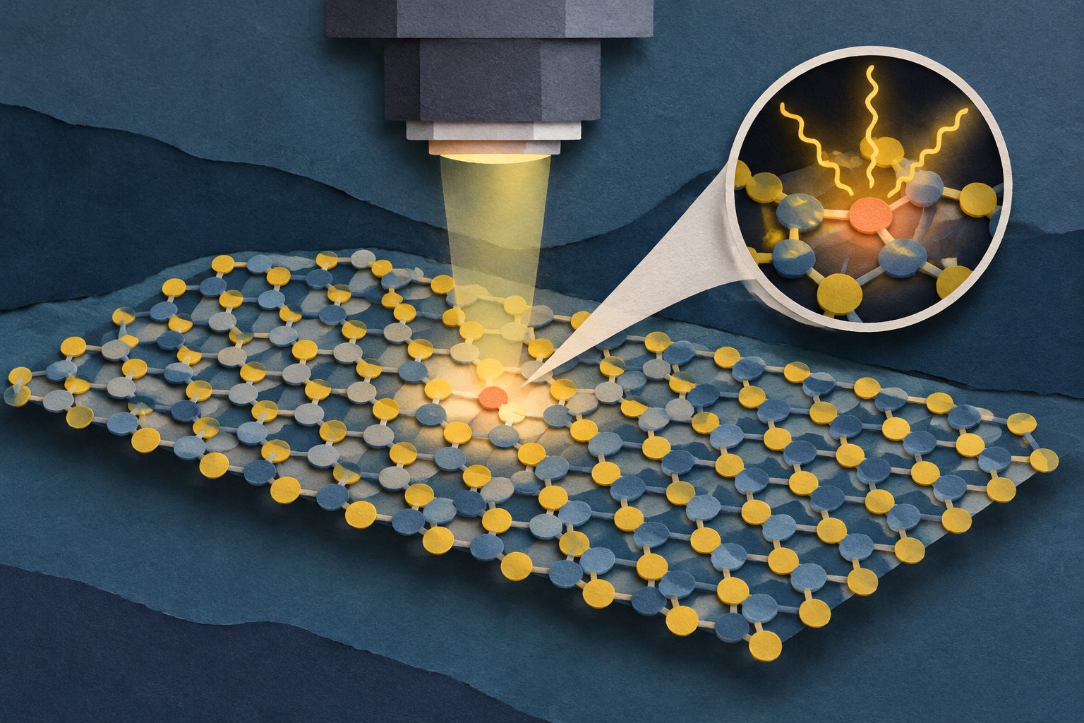
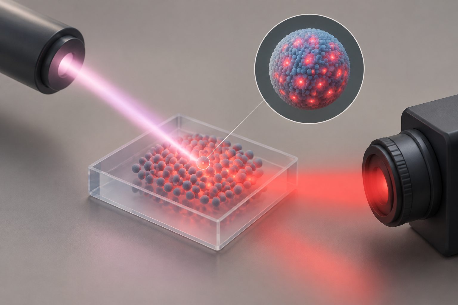
The images link specific atomic defects in MoS2 to excitons—bound pairs of electrons and holes—that produce distinct light emissions.
Using scanning tunnelling microscopy-induced luminescence, the researchers combined atomic-scale images with optical measurements of monolayer MoS2. A two-layer sheet of hexagonal boron nitride separated the MoS2 from a graphene substrate, helping preserve sharp emission from excitons and charged excitons, known as trions.
The measurements showed that sulfur vacancies and oxygen substitutions suppress the material’s usual exciton emission. By contrast, negatively charged carbon–hydrogen complexes produced defect-bound excitons about 200 millielectronvolts below the main MoS2 exciton, allowing the team to connect a specific atomic structure with a specific optical signature.
What the defects emit
The researchers used scanning tunnelling spectroscopy and scanning tunnelling microscopy-induced luminescence to examine individual defects in monolayer MoS2. Adding two layers of hexagonal boron nitride between the MoS2 and graphene increased the MoS2 band gap and extended defect charge-state lifetimes to about 30 picoseconds in the reported sulfur-vacancy comparison.
The setup detected sharp emissions from MoS2 excitons and several trion states. Their relative intensities varied on the nanoscale near local electrical-potential changes caused by nearby defects.
The team identified optical signatures for three defect types: sulfur vacancies, oxygen substitutions and negatively charged carbon–hydrogen complexes. Sulfur vacancies and oxygen substitutions reduced the usual MoS2 exciton emission but did not produce additional defect-related emission lines. The carbon–hydrogen complexes produced defect-bound excitons about 200 millielectronvolts below the main MoS2 exciton. Subnanometre-resolved maps showed that the defect emission was concentrated over roughly one to two nanometres and shifted in energy near the charged defect, in line with local band bending.
Why the atomic link matters
The work provides a direct link between the atomic structure of individual defects, their electronic states and the light they emit. That link addresses a central difficulty in studying defect-based light sources: optical measurements can show emission, but usually do not identify the exact atomic structure producing it.
By assigning an optical fingerprint to a particular defect type in MoS2, the study establishes a microscopic basis for engineering quantum emitters in two-dimensional materials more deliberately. The findings also show how separating MoS2 from graphene can preserve excitonic emission while retaining a configuration suitable for local electronic measurements.
Evidence and caveats
The evidence comes from atomic-scale scanning tunnelling microscopy and spectroscopy combined with scanning tunnelling microscopy-induced luminescence in monolayer MoS2 supported by bilayer hexagonal boron nitride and graphene. The researchers matched observed defect structures with their local electronic states and emission maps, and used the energy shifts near charged defects to support the interpretation of the carbon–hydrogen-complex emission as an exciton bound to an ionized acceptor-like defect.
The reported results concern the specific MoS2 heterostructures and defect types examined. The abstract and provided excerpts do not report how many individual defects were measured, how these emissions perform in an operating device, or whether the same defect assignments apply across other substrates or preparation conditions.
// Source
Nature Nanotechnology · 2026 · DOI: 10.1038/s41565-026-02314-x
Authors: Lysander Huberich, Yu Gu, Sotirios Papadopoulos, Chengye Dong, Joshua A. Robinson, Kenji Watanabe, Takashi Taniguchi, Oliver Gröning, Lukáš Novotný, Tingxin Li, Shiyong Wang, Bruno Schuler
Institutions: Shanghai Jiao Tong University, Centre National de la Recherche Scientifique, Université de Strasbourg, Empa, ETH Zurich, National Institute for Materials Science, Pennsylvania State University, Institut de Physique et Chimie des Matériaux de Strasbourg, Research Center for Materials Nanoarchitectonics