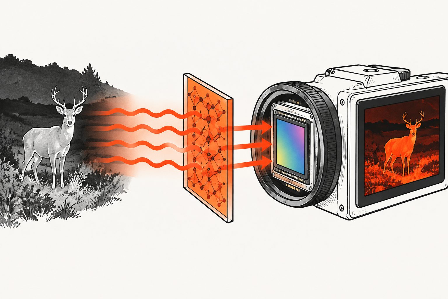
A pixelated array converts invisible heat signals into visible changes that a silicon-based camera can read.
The team integrated (PEA)2PbI4 perovskite films with silicon nitride membranes that absorb long-wave infrared light. Heating from the absorbed radiation changes the films' visible reflectance, allowing the infrared signal to be read optically rather than through electronic detector circuitry.
To preserve spatial detail, the researchers used structured probe illumination and built an array of thermally isolated membrane discs. The resulting pixelated imager reduced signal leakage between neighboring pixels and was read with a silicon-based CMOS camera.
Evidence and open questions
This is an experimental article reporting fabricated materials, membranes and pixelated imaging devices. The reported demonstration is at centimeter scale and focuses on 9.5-micrometer light, with sensitivity down to approximately 20 pW per square micrometer. The abstract does not provide details on imaging speed, long-term stability, manufacturing yield, operating conditions or performance against conventional infrared cameras, so the broader practicality of the platform remains to be established.
// Source
Light Science & Applications · 2026 · DOI: 10.1038/s41377-026-02442-y
Authors: Yanyan Li, Zheng Qian, Du Chen, Conrad A. Kocoj, Shunran Li, Renee Wu, Xiang Shi, Ralu Divan, David A. Czaplewski, Benjamin T. Diroll, Ming Chang Lu, Zhang Yugang, Shu Hu, Peijun Guo
Institutions: Yale University, Brookhaven National Laboratory, Argonne National Laboratory, Center for Nanoscale Materials, Center for Functional Nanomaterials