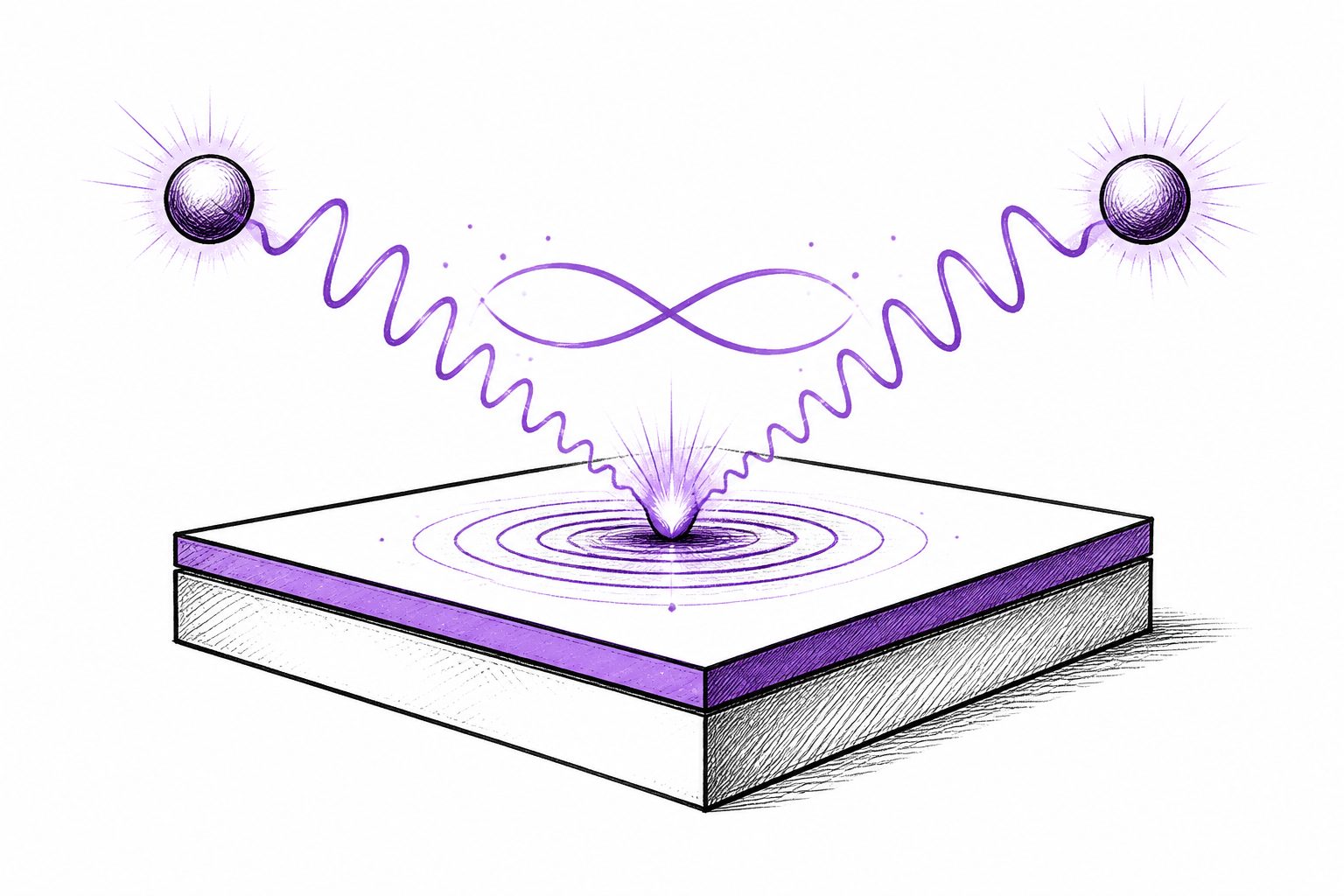
Computer models suggest that quantum wells and a patterned surface could generate photon pairs in a compact device about 0.5 micrometers thick.
The proposed device combines GaN quantum wells, whose built-in electric fields create a strong light response, with a dielectric metasurface designed to guide light into and out of the quantum-well region. The researchers used a quantum-optical theory that includes energy loss, fluctuations and noise, along with electromagnetic simulations and inverse design of the metasurface.
The calculations indicate that the structure can support parametric down-conversion, in which incoming light produces pairs of lower-energy photons with quantum correlations. The design works with light arriving straight onto the surface and targets photons in the telecommunications range, while having a total thickness of about 0.5 micrometers.
What the design predicts
The researchers proposed a source based on ScAlN/GaN multiple quantum wells integrated with an inverse-designed dielectric metasurface. Their analysis found that the wells have a strong second-order optical response in the near-infrared, and that the metasurface can be designed to improve three parts of the process: coupling the incoming pump light into the device, concentrating the optical field in the quantum wells, and letting the generated photons escape.
Using a Heisenberg–Langevin model that accounts for quantized fields, dissipation, thermal fluctuations and vacuum fluctuations, together with full-wave electromagnetic simulations, they calculated entangled-photon generation in the telecommunications band. The predicted biphoton generation rate is on the order of 10^10 per second from a structure about 0.5 micrometers thick.
Why a thin source matters
Telecommunications-band entangled photons are relevant to proposed quantum communication, sensing and information technologies. A compact source that combines the nonlinear material and light-guiding structure in one thin platform could be useful for integrated quantum photonic circuits.
The design also addresses challenges identified for nitride-based quantum-well structures, including strain-related growth problems and the difficulty of coupling normally incident light to transitions that respond mainly to electric fields perpendicular to the quantum wells.
// Source
Advanced Functional Materials · 2026 · DOI: 10.1002/adfm.78573
Authors: Jaeyeon Yu, Jewel Mohajan, Mikhail D. Tokman, Jackson Stewart, Anthony Rice, Sadhvikas Addamane, Oana Malis, Alejandro W. Rodriguez, Igal Brener, Raktim Sarma, Alexey A. Belyanin
Institutions: Purdue University West Lafayette, Texas A&M University, Princeton University, Ariel University, Sandia National Laboratories, Center for Integrated Nanotechnologies